Events

The 14th International Nanotechnology Exhibition & Conference (nano tech 2015)

Date&Time: January 28th - 30th, 2015, 10:00-17:00
Venue: Tokyo Big Sight, East Halls 4-6 & Conference Tower

----------------------------------------------------------------------------------------------------------

Researchers of Fraunhofer Institutes will have booths at nano tech 2015.

The following Fraunhofer Institutes will exhibit their latest developments:

  • Fraunhofer ENAS: Booth No. 5L-20
  • Fraunhofer IKTS: Booth No. 5N-18
  • Fraunhofer IMM: Booth No. 5J-02 (IVAM Booth)
  • Fraunhofer ISC: Booth No. 5N-17
  • Fraunhofer IWS: Booth No. 5Q-20 (Nanotech Kompetenz Zentrum Booth)

The detailed exhibition contents of each Fraunhofer Institutes, please see below.

------------------------------------

In addition to the booth exhibition, Fraunhofer researchers will give talks at the "Main Theater Presentation" on Jan.29th. 

"Main Theater Presentation - German Pavilion Nanotechnology ~ Made in Germany"

Date&Time: 2015.01.29. (Thu), 10:20-12:20, 13:00-16:45
Venue: Main Theater (East Hall 5)

11:45-12:00
"Applications of next generation nano-materials based on sol-gel processing and nano-/microtechnology“
Dr. Michael Popall (Fraunhofer ISC)

13:15-13:35
"Use of alumina nano-powders for schrinkage control in silver powder firing"
Dr. Markus Eberstein (Fraunhofer IKTS)

13:35-13:55
"Ressource efficient innovations based on nano technologies"
Prof. Dr. Thomas Geßner (Fraunhofer ENAS)

13:55-14:15
"Superhard carbon coatings for an improved energy efficiency"
Prof. Andreas Leson (Fraunhofer IWS)

14:15-14:35
"Nanostructured materials and processing techniques for Lithium Sulfur Batteries"
Prof. Stefan Kaskel (Fraunhofer IWS)

15:00-15:20
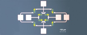
"Innovative 2D GMR sensors in monolithic integration for high-sensitivity applications"
Maria Almeida (Fraunhofer ENAS)

15:40-16:00
"Metal nano-inks for inkjet and aerosol printing"
Dr. Nikolai Trofimenko (Fraunhofer IKTS)

Exhibits

Modular high-temperature reactor for the continuous synthesis of nanoparticles

Fraunhofer ICT-IMM presents a novel, modular reactor for continuous flow synthesis of nanoparticles at elevated temperatures. The reactor is capable of performing liquid-phase reactions at temperatures of up to 400 °C, common hot-injection synthesis protocols for the synthesis of nanomaterials can now be transferred from batch to continuous. Examples include organo-metallic syntheses as used for CdSe quantum dots (QDs), Pt and other metal nanoparticles, or oxide materials.

picture upper: Polylactide composite nanoparticles
picture down: CdSe quantum dots

About Fraunhofer IMM

Within the research area of Nanoparticle Technologies our scientists carry out research and development with

  • the production and characterization of nanoparticles with diverse attributes and application possibilities in medicine, pharmacy as well as in the consumer goods industry.
  • bio-nano interfaces, the fabrication of Micro- and Nanocolloids with engineered interface for specific applications as well as the development and synthesis of intelligent polymer-based particles.
  • analyzing nanoparticles of different materials under various conditions.

Other key competences are Decentralized and Mobile Energy Technology, Continuous Chemical Engineering, Medical Probes and Technical Sensors as well as Microfluidic Analysis Systems.

Contact

Fraunhofer ICT-IMM
Carl-Zeiss-Str. 18-20
55118 Mainz, Germany

Dr. Ralph Sperling
Head of Nanoanalytics Group
Phone: +49-6131-990-246
E-Mail: Ralph.Sperling@imm.fraunhofer.de

Exhibits

REACH and RoHS compliant thick-film paste portfolio

Power electronics is becoming a key technology for a rising number of products and systems due to a global trend to green energy and the establishment of electric mobility.
Our researchers now focus on high-performance and high-thickness screen-print pastes for AlN and Si3N4 as excellent buildup materials for power electronics and assemblies.
New additives, adopted organic vehicle, and modified manufacture technologies are used to tune properties such as the temperature coefficient of the resistor and adhesion strengths of solder joints. Our “Pastemeleon” awaits you on the booth!


Environmentally friendly water-based nanoparticle-printing inks and multilayerbased microsystems

Direct writing technologies like inkjet or aerosol printing for silver, copper, gold and platinum inks are promising methods to print contactlessly thin functional layers in order to realize optimized microelectronic devices such as circuit paths or heaters easily.
Fraunhofer IKTS develops those environmentally friendly water-based nanoparticleprinting inks for polymeric and ceramic substrates. The application of nanoinks for the wiring of surface mounting devices on low-temperature co-fired ceramics (LTCC) as well as extremely robust ceramic multilayer acceleration sensors are examples of new technologies presented on the booth.

About Fraunhofer IKTS

The Fraunhofer IKTS conducts applications-oriented research in the field of high-performance ceramics. As research and technology service provider, the German institution develops ultramodern high-performance ceramic materials, industrially relevant manufacturing processes, prototype components and systems in complete production lines, through to pilot-scale production. At its heart are market-viable ceramic solutions for mechanical and plant engineering, energy and environmental technology, optics, medical technology as well as electronics and microsystems technology. The research portfolio is expanded with expertise in materials diagnostics and testing. The test procedures in the fields of acoustics, electromagnetics, optics, microscopy and laser technology contribute substantially to the quality assurance of customer’s products and systems. Nanomaterials often play the key role in innovations.

Contacts

Fraunhofer Institute for Ceramic Technologies and Systems IKTS
Winterbergstrasse 28, 01277 Dresden, Germany
www.ikts.fraunhofer.de

Dr. Markus Eberstein
Phone +49 351 2553-7518
markus.eberstein@ikts.fraunhofer.de

Dr. Nikolai Trofimenko
Phone +49 351 2553-7787
nikolai.trofimenko@ikts.fraunhofer.de

Exhibits

Magnetic field sensor

Fraunhofer ENAS will present a new type of spintronic magnetic field sensor with two-dimensional vector resolution for contact-free measurement of distances, speeds, and angles. The magnetic field sensor's functionality is based on the physical giant magnetoresistance (GMR) effect. Technologies such as PVD and plasma etching processes are employed for fabrication. Thanks to those micro- and nanotechnologies used, it is possible to attain a very high signal-to-noise ratio, very short response times, a high degree of miniaturization, and a very low level of energy consumption. The GMR sensor is also bio-compatible. Conceivable applications range from the aerospace and the automobile industry to the very latest devices in medical engineering.

Integration of Carbon Nanotubes and applications

Fraunhofer ENAS investigates the integration of nanomaterials like carbon nanotubes (CNT) and their application in electronics and sensors with industrial compatible technologies. Therefore we focus on wafer level technologies for CNT material fabrication as well as material conditioning, the assembling or site-selective growth of CNTs, contact formation and fabrication of CNT-based devices. Target applications are CNT based high frequency field effect transistors for communication applications as well as ultra-sensitive and miniaturized sensors.

Focus of R&D activities:

  • Waferscale technologies for nanomaterial integration
  • Integration of CNTs into interconnect systems and MEMS/NEMS
  • CNT FETs for high frequency analogue applications
  • CNT based sensors (e.g. piezoresistors in N/MEMS)
  • Chemical vapour deposition of CNTs on wafer scale
  • Wafer scale dielectrophoretic assembly of CNTs

Low-temperature Bonding

Fraunhofer ENAS offers these technologies for low-temperature wafer bonding:

  • Room-temperature bonding by using reactive nano scale multilayer
  • Anodic bonding (glass/Si)
  • Direct bonding (glass/glass; glass/Si; SiSi)
  • Adhesive bonding (SU-8; BCB)
  • Solid-liquid interdiffusion bonding (CuSn)
  • Thermo-compression bonding

About Fraunhofer ENAS

The Fraunhofer Institute for Electronic Nano Systems ENAS focuses on smart systems integration by using micro and nano technologies and provides services in:

  • Development, design and test of MEMS and NEMS (micro and nano electro mechanical systems)
  • Wafer level packaging of MEMS and NEMS, wafer bonding, low temperature bonding
  • Metallization and interconnection systems for micro and nano electronics as well as 3D integration
  • Adaptive printing technologies inclusively material development and characterization
  • Reliability and security of micro and nano systems.

In Sendai, the Fraunhofer Project Center “NEMS/MEMS Devices and Manufacturing Technologies at Tohoku University” was founded as a platform for common research and development activities of Tohoku University and Fraunhofer ENAS. The project center is run to the benefit of both partners as a vehicle for R&D cooperation, technology transfer as well as training and education programs.

Contacts

Fraunhofer Institute for Electronic Nano Systems ENAS
Technologie-Campus 3
09126 Chemnitz, Germany
www.enas.fraunhofer.de

Prof. Dr. Thomas Gessner
Director
Phone: +49 371 45001-100
e-mail: thomas.gessner@enas.fraunhofer.de

Jörg Frömel
Phone: +49 371 45001-260
e-mail: joerg.froemel@enas.fraunhofer.de

Exhibits

Fraunhofer ISC will present test objects, demonstrators and functional prototypes of applications based on our nano-materials:

  • Low-k and high-k dielectrics and passivation for electrical interconnection technology
  • Low and high refractive optical matrices for integrated optics and photonics
  • Ultra barrier materials for packaging of food, photonics, photovoltaic and display-technology
  • Functional abrasion resistant coatings
  • Piezo materials for sensing and actuating devices
  • Inorganic oxidic multilayers for antireflection and filtering
  • Functional nano-particles for multifunctional layers and devices
  • Electrolytes and nano-electrodes for batteries and super-capacitors
  • Printable metal-oxides for transparent electronics
  • Scattering layers to be used in photovoltaic in OLED applications

Further-on will be presented new approaches for printing of integrated circuits based on ISC- nano-materials as well as new processes based on two-photon absorption technology and ISC-nano-materials.

About Fraunhofer ISC

The Fraunhofer ISC focuses on developing materials with new or enhanced properties for customized applications, and on methods of manufacturing and processing such materials.
The business success of our customers and partners is our overriding aim.

The institute's core competencies are acquired through self-financed fundamental research and elaborated with the market requirements in view.

Core competencies are:

  • Synthesis of inorganic and hybrid functional materials, ceramics and glass, preferably using techniques involving chemical nanotechnology
  • Material processing techniques for the production of suspensions, powders, fibers, coatings, microstructures and composites, and building functional models
  • Material characterization, analysis and optimization, and procedures for monitoring high-temperature processes

Contacts

Fraunhofer ISC
Neunerplatz 2, 97082
Würzburg, Germany

Dr. Michael POPALL
Head of ISC International
Phone: (+)49 - 931 4100 522
Fax: (+)49 - 931 4100 559
michael.popall@isc.fraunhofer.de


Gerhard DOMANN
Head of Competence Unit Optics & Electronics
Phone: (+)49 - 931 4100 551
Fax: (+)49 - 931 4100 559
gerhard.domann@isc.fraunhofer.de