Fraunhofer ENAS
Inductive bonding – A new bonding method in microsystems technology
The Fraunhofer Institute for Electronic Nano Systems ENAS is developing a new bonding technology for microsystems in cooperation with Chemnitz University of Technology and SHINKO ELECTRIC INDUSTRIES CO., LTD. The chip-level inductive bonding process will be presented for the first time at MEMS Sensing & Network System 2022 in Tokyo.
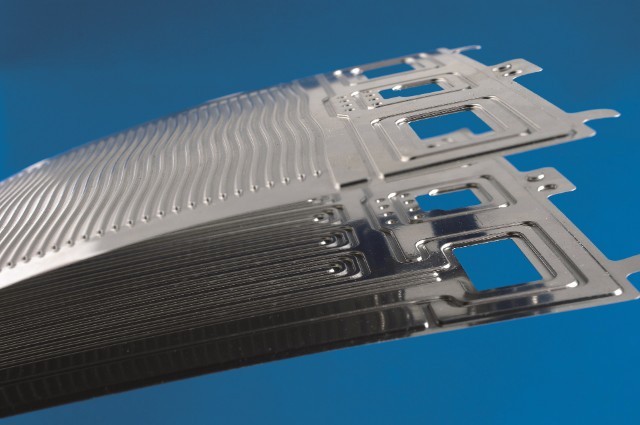
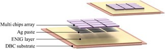
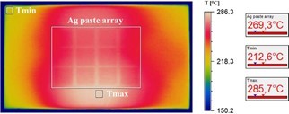
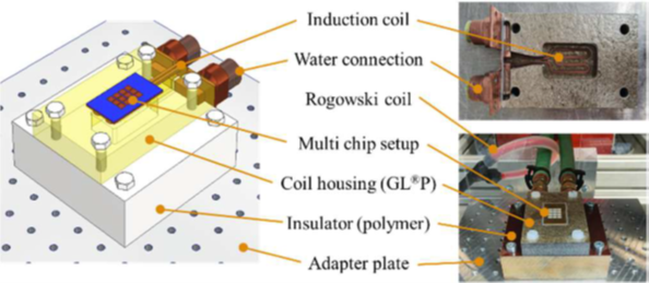
Inductive joining is a technology that has so far mainly been used only for macroscopic components, such as steel tubes or car doors. Fraunhofer ENAS, together with Chemnitz University of Technology and the Japanese company SHINKO, is now developing a process that enables inductive bonding on the micr o level for the first time. A bonding process based on sintering paste with silver micro particles was developed for the mechanical surface contacting of chips on DBC (direct bonded copper) substrates.
At the trade show MEMS Sensing & Network Systems in Tokyo Big Sight from Jan 26 until 28, the process will be presented at the joint booth of Tohoku University and Fraunhofer ENAS (hall 2, booth 2D-05).
A paper on inductive chip bonding can be requested under the following contact: events@enas.fraunhofer.de (Subject: Paper inductive bonding).
For more information, please refer the press release (pdf).