Event

nano tech 2017

Date&Time: February 15-17, 2017, 10:00-17:00
Venue: Tokyo Big Sight, East 4・5・6 Hall & Conference Tower
Entrance Fee: 3,000 Japanese Yen(Free admission with online registration)
--------------------------------------------------------------------------------------------------------

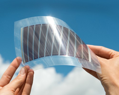
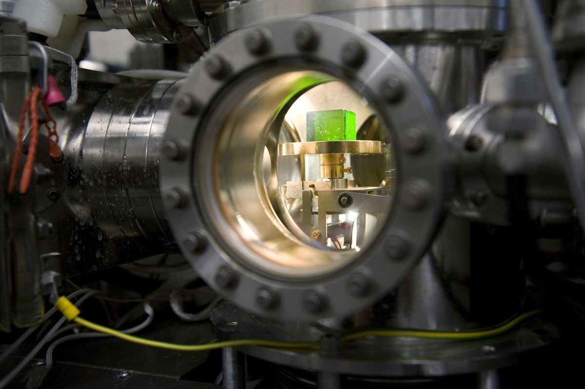
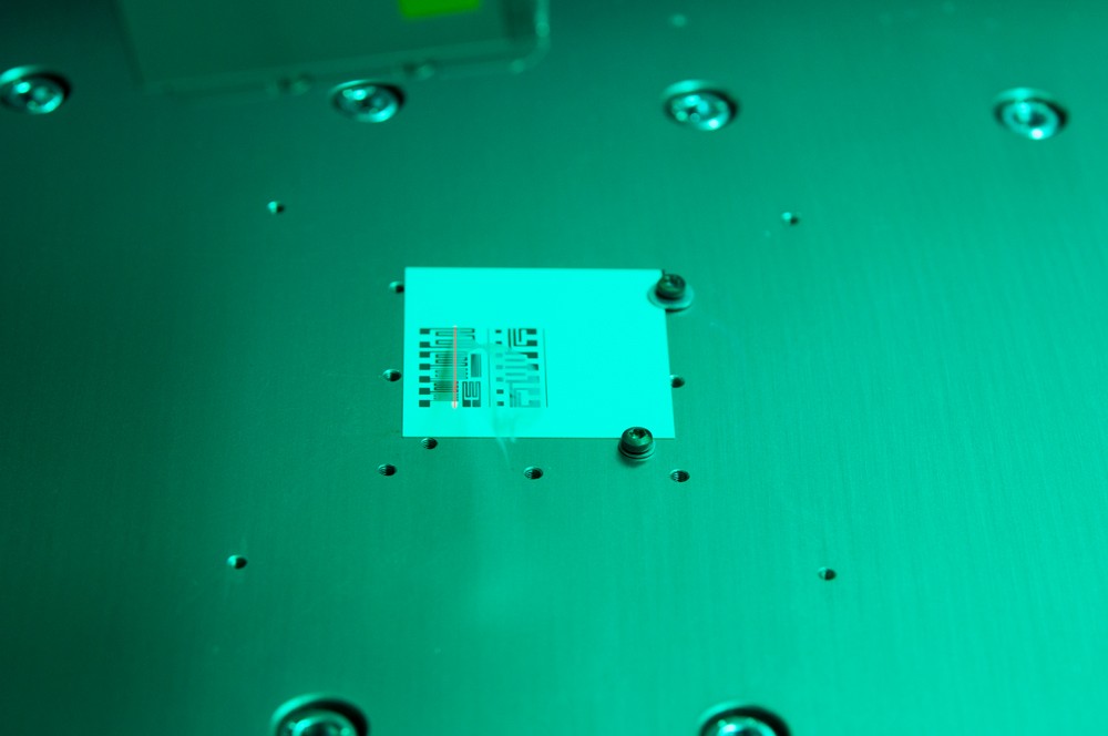
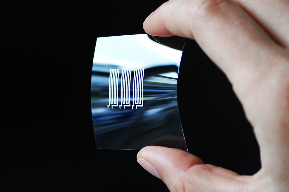
Following institutes are going to introduce their latest research results:

Fraunhofer Institute for Ceramic Technologies and Systems IKTS: 5J-14
Fraunhofer Institute for Material and Beam Technology IWS: 5J-14
Fraunhofer Institute for Organic Electronics, Electron Beam and Plasma Technology FEP: 5J-14
Fraunhofer Institute for for Reliability and Microintegration IZM-ASSID: 5J-14
Fraunhofer Institute for Silicate Research ISC: 5R-18

Exhibits

At nano tech 2017 Fraunhofer ISC will present test objects, demonstrators and functional prototypes of applications based on our nano-materials:

- Ultra-barrier materials for packaging, photovoltaic and displays
- Functional coatings
- Functional nano particles
- Nano-analytics
- Micro optics and micro electronics
- Dielectrics and passivation for electrical interconnection technology
- Diffractive optical matrices for integrated optics and photonics
- Two-photon absorption (TPA), two-photon polymerization (2PP) and nano-imprint technology
- New approaches for printing of integrated circuits
- Printable metal-oxides for transparent electronics
 

About Fraunhofer ISC

The Fraunhofer ISC focuses on developing materials, coatings and nano particles with new or enhanced properties for customized applications, and on methods of manufacturing and processing such materials. The business success of our customers and partners is our overriding aim. The institute's core competencies are acquired through self-financed fundamental research and elaborated with the market requirements in view.

Core competencies are:
- Synthesis of inorganic and hybrid functional materials, ceramics and glass, preferably using techniques involving chemical nanotechnology
- Material processing techniques for the production of suspensions, powders, fibers, coatings, microstructures and composites, and building functional models
- Material characterization, analysis and optimization, and procedures for monitoring high-temperature processes 


Contact

Fraunhofer ISC
Neunerplatz 2, 97082
Würzburg, Germany

Dr. Michael POPALL
Head of ISC International
Phone: (+)49 - 931 4100 522
Fax: (+)49 - 931 4100 559
michael.popall@isc.fraunhofer.de 

Exbisits

3D printed electronics on large structural components


Researchers of Fraunhofer IKTS have successfully combined ceramic thick-film and direct writing technologies with laser sintering to directly apply conductors, resistors or heaters on metal substrates.

The new process combination, based on new paste and nanoink compositions, can be used, e.g., to directly integrate sensors for structural health monitoring of large metal components, such as power rotors and roller bearings of turbines, without brazing and adhesive bonding. The new solution can overcome the disadvantages of conventional hybrid sensors: The IKTS 3D printed electronics are resistant against aggressive media, operating temperatures of more than 200 °C, as well as high acceleration forces.


Meet our experts for individual discussions at our booth or attend their presentations:

February 15, 2017, 13:50 – 14:10 (presentation), Booth 5J-14
“Nanoink manufacturing and curing: challenges and solutions” (Mihails Kusnezoff)

February 16, 2017, 14:10 – 16:10 (open workshop), Booth 5J-14
“New pastes for printed electronics on AlN, LTCC, and Solar Cells”
(in English with consecutive Japanese translation, free-of-charge)

February 17, 2017, 11:10 – 11:30 (presentation), Booth 5J-14
“Nano powders as a key feature in contemporary Solar Cell Metallization Pastes” (Markus Eberstein)

For more information please have a look at our Homepage.