Events

nano tech 2016

Date&Time: January 27-29, 2016, 10:00-17:00
Venue: Tokyo Big Sight, East 4・5・6 Hall
Entrance Fee: free
--------------------------------------------------------------------------------------------------------

Following institutes are going to introduce their latest research results at the booths within German Pavilon:

  • Fraunhofer Institute for Electronic Nano Systems ENAS: 5J-14
  • Fraunhofer Institute for Ceramic Technologies and Systems IKTS: 5K-12
  • Fraunhofer Institute for Silicate Research ISC: 5L-16
  • Fraunhofer Institute for Material and Beam Technology IWS: 5J-13

Furthermore, researchers from Fraunhofer ENAS, FEP, IKTS and IWS are going to have talks at the SAXONY! joint booth (5M-13) during the exhibition. Please see the details here

Exhibits

Fraunhofer ISC will present test objects, demonstrators and functional prototypes of applications based on our nano-materials:

  • Dielectrics and passivation for electrical interconnection technology
  • Diffractive optical matrices for integrated optics and photonics
  • Piezo materials for sensing and actuating devices
  • Ultra-barrier materials for packaging, photovoltaic and displays
  • Functional coatings: antireflective, abrasion resistant 
  • Electrolytes and nano-electrodes for batteries and super-capacitors
  • Printable metal-oxides for transparent electronics
  • New approaches for printing of integrated circuits
  • Two-photon absorption technology (TPA)

About Fraunhofer ISC

The Fraunhofer ISC focuses on developing materials with new or enhanced properties for customized applications, and on methods of manufacturing and processing such materials. The business success of our customers and partners is our overriding aim. The institute's core competencies are acquired through self-financed fundamental research and elaborated with the market requirements in view.

Core competencies are:

  • Synthesis of inorganic and hybrid functional materials, ceramics and glass, preferably using techniques involving chemical nanotechnology
  • Material processing techniques for the production of suspensions, powders, fibers, coatings, microstructures and composites, and building functional models
  • Material characterization, analysis and optimization, and procedures for monitoring high-temperature processes

Contact

Fraunhofer ISC
Neunerplatz 2, 97082 
Würzburg, Germany

Dr. Michael POPALL
Head of ISC International
Phone: (+)49 - 931 4100 522
Fax: (+)49 - 931 4100 559
michael.popall@isc.fraunhofer.de

Exhibits

Fraunhofer IKTS offers solutions on high-performance screen-print pastes, nanoinks and powders towards the next generation of power electronics and advanced functional elements.

Highlights:

Power electronics is becoming a key technology for a rising number of products and systems due to a global trend to green energy. For increasing local current transport and storage, new low-cost converting equipment is needed. Key challenges facing R&D nowadays are system integration, higher energy density, better heat dissipation, higher robustness and reliability as well as optimized passive components.

High performance thick-film pastes for AlN, Si3N4, and warpage-free LTCC

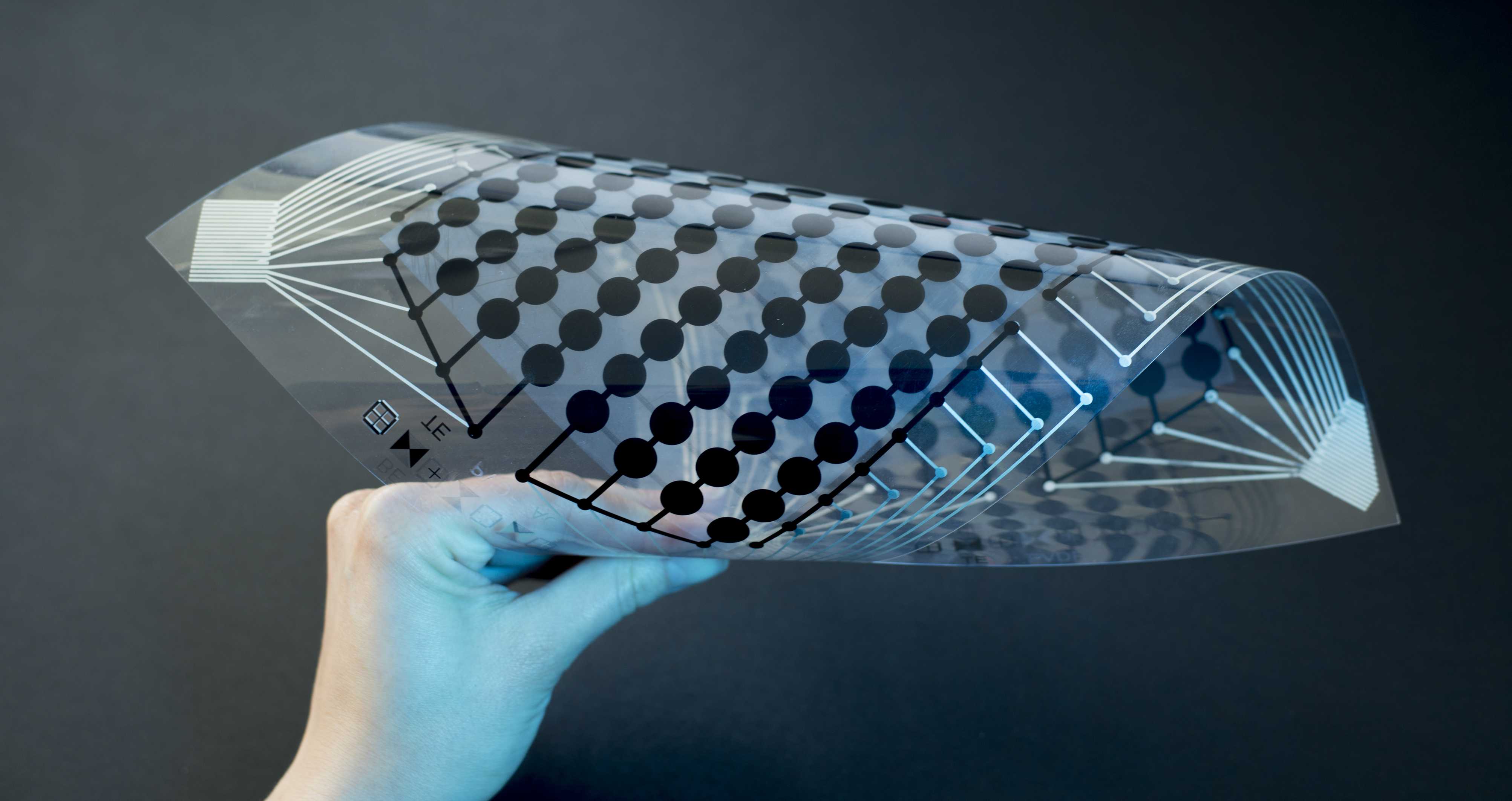
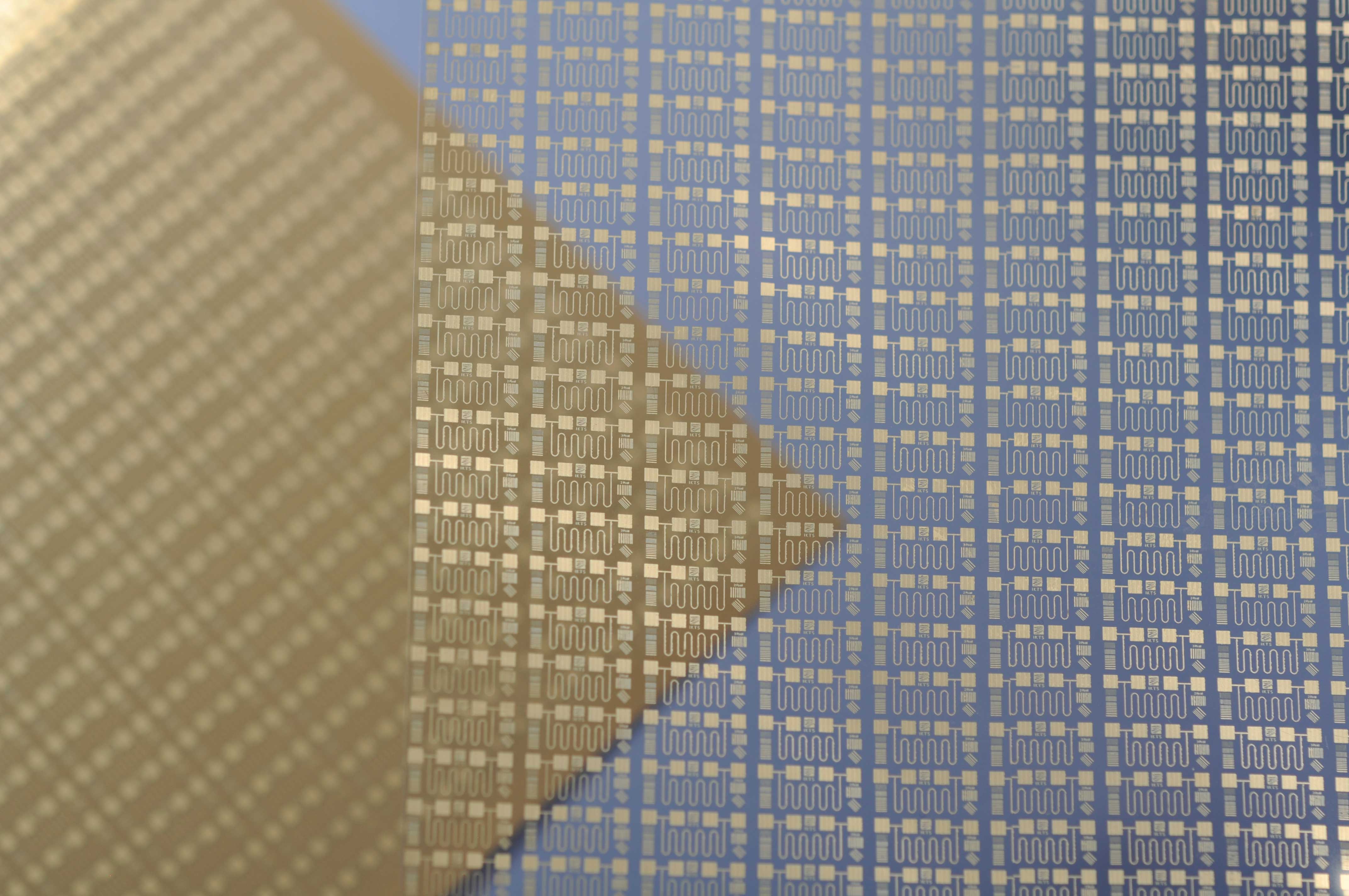
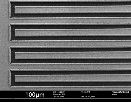
Fraunhofer IKTS presents screen-print pastes with a broad variety in properties for AlN and Si3N4 substrates. Screen-print thick-film technology offers a series of advantages in the design of electronic circuits: direct printing of high-performance resistors and conductors, embedding of single and power tracks, suitable for high-voltage- and high-frequency applications, realization of multilayer circuits, double-sided and any-shape usage. A growing number of customers stands for the quality of IKTS products.

The Low Temperature Co-fired Ceramics (LTCC) multilayer technology has been a technology driver in microelectronic packaging since two decades. However, due to a limited chemical match between LTCC tape and the metallization, co-firing was often accompanied by undesired warpage effects and expensive post-firing processes had to be applied. IKTS researchers developed a series of new pastes especially dedicated to the co-firing process. The pastes match the sintering shrinkage of the tape precisely and enable low-cost sintering of highly integrated LTCC controller and sensor modules.

Nanoparticle-based metal inks

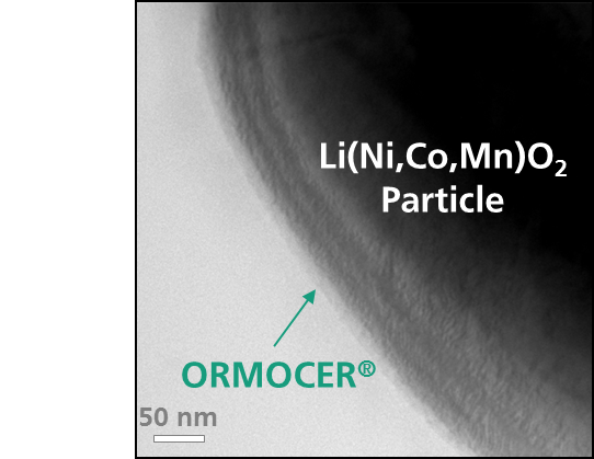
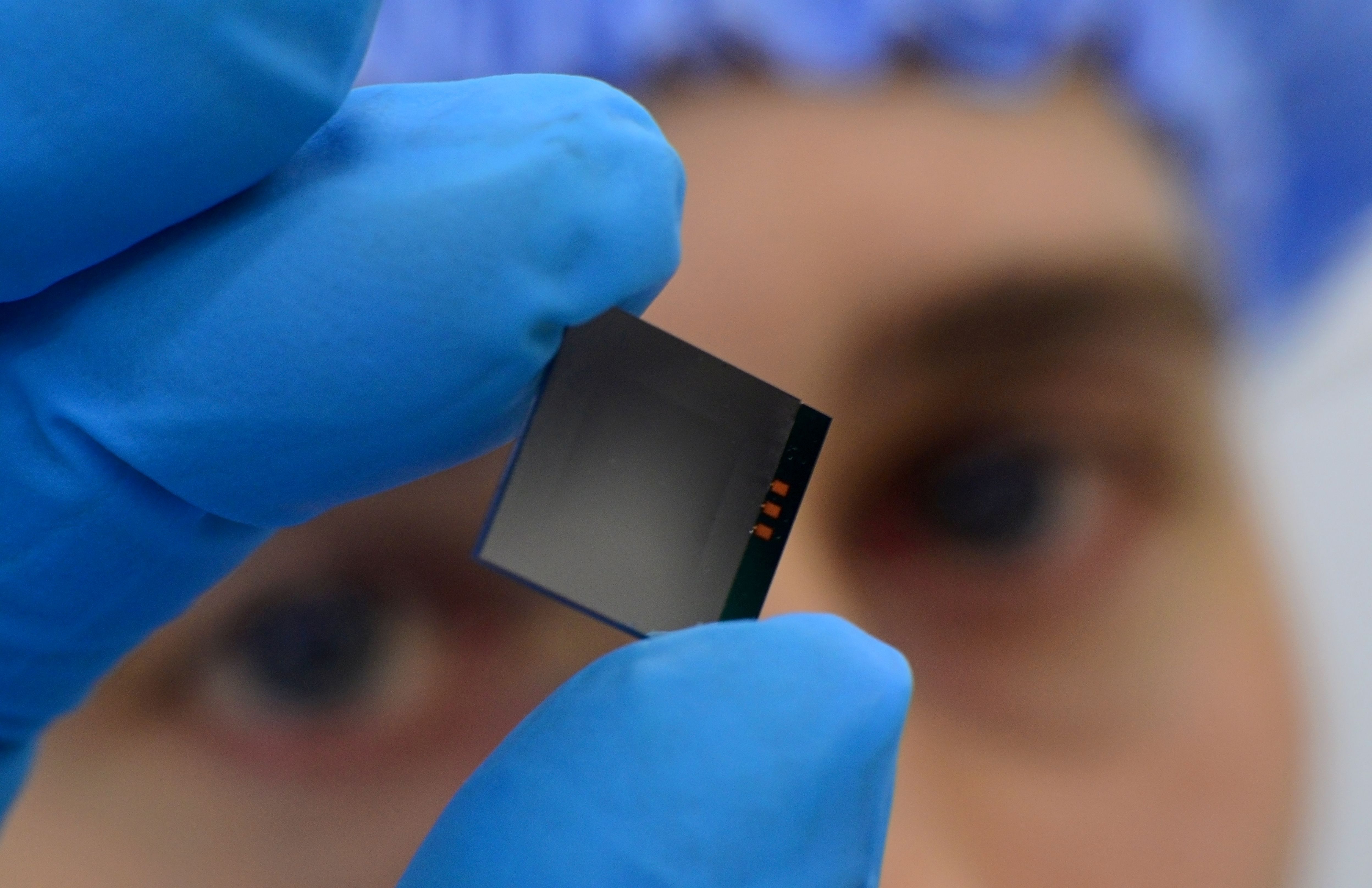
Based on experience with mixed oxides (perovskites, spinels, fluorites), noble metals and carbon-based materials different types of novel water-based metal nanoparticle (Ag, Au, Pt, Cu) printing inks, mixed oxides and slurries were developed, that are used in electrochemical storage and conversion devices as well as microsystems. All developed products have been adjusted for proper coating technologies like tape casting or direct writing methods. Extensive experience and outstanding technical equipment allow to satisfy the complex requirements in applications such as fuel cells, Li-ion batteries and supercapacitors as well as chemical and physical sensors.

For nanoinks the influence of different parameters (pH, concentration of metal, temperature and nature of a surfactant) on particle size distribution, viscosity and yield were investigated. The optimization of manufacturing steps with focus on volume manufacturing processes (up-scaling for powders, paste and inks production, applications for screen and ink-jet printing, cost effective co-sintering or low-temperature sintering etc.), reproducibility and cost reduction is an important factor for actual and further developments. With the help of the developed materials electronic components like antenna, heater and thermocouples as well as more complex components such as electrochemical cells, high-temperature fuel cell stacks, sensors, battery and capacitor electrodes are built up and qualified for system integration.

About Fraunhofer IKTS

The Fraunhofer IKTS conducts applications-oriented research in the field of high-performance ceramics. As research and technology service provider, the German institution develops ultramodern high-performance ceramic materials, industrially relevant manufacturing processes, prototype components and systems in complete production lines, through to pilot-scale production. At its heart are market-viable ceramic solutions for mechanical and plant engineering, energy and environmental technology, optics, medical technology as well as electronics and microsystems technology. The research portfolio is expanded with expertise in materials diagnostics and testing. The test procedures in the fields of acoustics, electromagnetics, optics, microscopy and laser technology contribute substantially to the quality assurance of customer’s products and systems. Nanomaterials often play the key role in innovations.

Contacts

Fraunhofer Institute for Ceramic Technologies and Systems IKTS
Winterbergstrasse 28, 01277 Dresden, Germany
www.ikts.fraunhofer.de

Dr. Markus Eberstein
Phone +49 351 2553-7518
markus.eberstein@ikts.fraunhofer.de

Dr. Nikolai Trofimenko
Phone +49 351 2553-7787
nikolai.trofimenko@ikts.fraunhofer.de

Exhibits

MEMS loudspeaker utilizing metallic glass membrane and deposited magnet

The silicon-based MEMS loudspeaker consists of a metallic glass membrane with dispensed magnetic paste and electroplated micro coil. This is the world’s first approach of a MEMS speaker with electrodynamic actuation that is completely fabricated on wafer-level with no need to attach bulk magnets manually. Metallic glasses exhibit high strength, large elastic limit and no material fatigue.

Mirau interferometer for vertically integrated array-type Mirau-based OCT system for early diagnostics of skin pathologies

The Mirau interferometer, consists of a doublet of array of micro lenses, an array of actuated micro mirror, a focus-adjustment spacer and a beam splitter plate. The batch fabrication can be achieved through optimized MOEMS process which gathers similar components onto specialized wafers such as Si or glass. The 5-stack demonstrator is anodic bonded at bonding temperature lower than 360 °C.

Nanoporous metal for micro energy storage systems

For achieving high values of electrical capacitance in supercapacitor architectures, electrodes with large surface-to-volume ratio are needed. Fraunhofer ENAS is applying nanoporous metal within a simple and MEMS compatible process. Fabricated nanoporous gold structures can be applied as electrodes for micro double-layer capacitors (supercapacitors).

Solid-liquid interdiffusion bonding (SLID) at wafer-level

SLID bonding is realized by a short liquid phase of one low melting metal and the immediate solidification caused by diffusion and intermixing with a second, high melting metal (Solid-Liquid Interdiffusion – SLID). Ideally a stable intermetallic phase is generated. Depending on the low melting material some of the combinations allow a process temperature lower than 300 °C.

Aerosol jet printing

Aerosol Jet is a non-contact direct-writing technology which allows the deposition of various functional materials such as particle inks, polymers, etchants and paste like fluids. By combination of both pneumatic atomizers, mixing of different materials becomes possible. With this unique mixing process, i.e. graded depositions of functional layers can lead to new applications.

About Fraunhofer ENAS

Smart Systems Integration by using Micro and Nano Technologies

Fraunhofer ENAS is your partner for applied research in micro and nano systems technology.

  • Development, design and test of MEMS and NEMS
  • Wafer level packaging and low-temperature wafer bonding
  • 3D integration as well as metallization and interconnection systems for micro and nano electronics
  • Adaptive printing technologies inclusively material development and characterization
  • Reliability and security of micro and nano systems.

Fraunhofer ENAS cooperates closely with the Fraunhofer Project Center “NEMS/MEMS Devices and Manufacturing Technologies at Tohoku University” and the WPI-AIMR at the Tohoku University in Sendai, Japan.

Contact

Fraunhofer Institute for Electronic Nano Systems ENAS

Technologie-Campus 3,
09126 Chemnitz
Germany

Director:
Prof. Dr. Thomas Gessner
Phone: +49-371-45001-100
E-Mail: thomas.gessner@enas.fraunhofer.de
Internet: www.enas.fraunhofer.de